Premium listings
-
 Prefabricated And Integrated Foldable Container HouseConstruction - Building Materials - QHCC - Hong Kong - August 20, 2025 - 4000.00 Dollar US$
Foldable Prefabricated House Overall Size:2438*5900*2620mm Top frame :Crossbeam 5480*2.0-2 2138*2.0-2, 210*150 corner piece-4, purlin 100*40*1.0, insulation cotton, iron sheet color steel plate 0.35mm, top guide rail, 0.25mm831 ceiling. Bottom frame ...
-
 Prefabricated And Integrated HouseConstruction - Commercial - QHCC - Hong Kong - July 29, 2025 - 6350.00 Dollar US$
Mobile house-foldable house-Space capsule Product presentation Double wing expansion box room can be used by multiple up and down left and right splicing, to adapt to regional strength, only simple tools in the installation process, beautiful appeara...
check valve wafer Photos Catalog - page 15 - WorldBid B2B Market
-
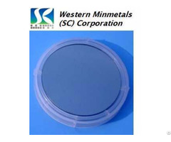
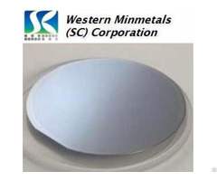
 Gallium Arsenide Gaas Un Doped Semi Insulating Wafer Substrate 2 3 4 6 At WmcComponents - Other - Western Minmetal (SC) Corporation - China - December 24, 2017 - 1.00 Dollar US$
Diameter: 50.8+/-0.2mm, 76.2+/-0.3mm, 100+/-0.5mm 150+/-0.5mm Growth Method: VGF Dopant: None Thickness: 350-625+/-25um Crystal Orientation: <100>+/-0.5degree or +/-2.0degree Orientation Flat / Length: as SEMI, 16+/-1, 22+/-2 or 32+/-1 mm Ident...
-
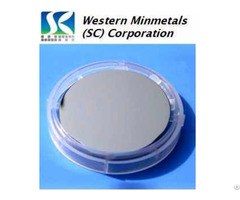
 Gallium Arsenide Gaas Si Doped Wafer 2 3 4 At Western Minmetals Sc CorporationComponents - Other - Western Minmetal (SC) Corporation - China - December 24, 2017 - 1.00 Dollar US$
Diameter: 50.8+/- 0.2, 76.2+/-0.3, 100+/-0.3 mm Dopant: Silicon Conduct Type: SC/N Growth Method: VGF Thickness: 220-350+/-20 um Crystal Orientation: <100>+/-0.5degree O rientation Flat / Length: 16+/-1, 22+/-1, 32+/-1 mm Identification Flat / ...
-
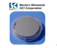
 Gallium Arsenide Gaas Zn Doped Wafer 2 3 4 At Western Minmetals Sc CorporationComponents - Other - Western Minmetal (SC) Corporation - China - December 24, 2017 - 1.00 Dollar US$
Diameter: 50.8+/- 0.2, 76.2+/-0.3, 100+/-0.3 mm Dopant: Zinc Conduct Type: SC/P Growth Method: VGF Thickness: 220-350+/-20 um Crystal Orientation: <100>+/-0.5degree O rientation Flat / Length: 16+/-1, 22+/-1, 32+/-1 mm Identification Flat / Len...
-
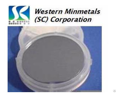
 Gallium Phosphide Gap Single Crystal Wafer 2 At Western Minmetals Sc CorporationComponents - Other - Western Minmetal (SC) Corporation - China - December 24, 2017 - 1.00 Dollar US$
Diameter: 50.8+/- 0.2 mm Dopant: None / Sulphur Conduct Type: SC/P Growth Method: LEC Thickness: 300+/-20 um Crystal Orientation: <111>+/-0.5degree O rientation Flat / Length: as SEMI Identification Flat / Length: as SEMI Orientation / Identifi...
-
 Gallium Antimonide Gasb Single Crystal Wafer 3 4 At Western Minmetals Sc CorporationComponents - Other - Western Minmetal (SC) Corporation - China - December 24, 2017 - 1.00 Dollar US$
Diameter: 76.2+/- 0.2, 100+/-0.2 mm Dopant: None / Tellurium / Zinc Conduct Type: N / P Growth Method: LEC Thickness: 625+/-25, 1, 000+/-25 um Crystal Orientation: <100> <111>+/-0.5degree O rientation Flat / Length: as SEMI Identification...
-
 Indium Phosphide Inp Single Crystal Wafer 2 3 At Western Minmetals Sc CorporationComponents - Other - Western Minmetal (SC) Corporation - China - December 24, 2017 - 1.00 Dollar US$
Diameter: 50.8+/- 0.2, 76.2+/- 0.2 mm Dopant: None / Sulphur / Ferrum / Zinc Conduct Type: N / P Growth Method: LEC Thickness: 200-2, 000+/-5 or +/-10 um Crystal Orientation: <100> <111> Orientation Flat / Length: as SEMI Identification F...
-
 Indium Antimonide Insb Single Crystal Wafer 2 At Western Minmetals Sc CorporationComponents - Other - Western Minmetal (SC) Corporation - China - December 24, 2017 - 1.00 Dollar US$
Indium Antimonide (InSb) Single Crystal Wafer 2’’ at Western Minmetals (SC) Corporation Diameter: 50.8+/- 0.2 mm Dopant: None / Tellurium / Germanium Conduct Type: N / P Doping Level: > 2E18 /cm2 Growth Method: LEC Thickness: 500+/-25 um Warp: <...
-
 Indium Arsenide Inas Single Crystal Wafer 2 3 At Western Minmetals Sc CorporationComponents - Other - Western Minmetal (SC) Corporation - China - December 24, 2017 - 1.00 Dollar US$
Diameter: 50.8+/- 0.2, 76.2+/- 0.2 mm Dopant: None / Sulphur / Zinc Conduct Type: N / P Doping Level: > 2E18 /cm2 Growth Method: LEC Thickness: 500+/-25 um Warp: < 15 um Crystal Orientation: <100>+/-2degree, <111>+/-2degree, Alpha90...
-
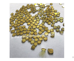 Diamond Wafer For Cutting ToolsCutting Tools - more super hard product comapny - China - January 28, 2018 - 0.10 Dollar US$
Single crystal 6.0mm synthetic HPHT diamond dresser� ��plate Features: Hardnes s and wear resistance, diamond is combined by covalent bond has a saturated and directional crystal, so it has a very high hardness and wear resistance, is now known as the ...
-
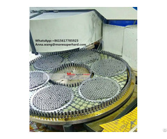
 Silicon Wafer Back Side Diamond Grinding WheelEquipment - Abrasives - more super hard product comapny - China - April 17, 2018 - 1.00 Dollar US$
Back Grinding Wheels Back Grinding Wheels Are Used For The Thinning And Fine Grinding Of The Silicon Wafer. Name: Diamond Backgrinding Wheel Application: Silicon WaferDiamond Back Grinding Wheels Are Used For Silicon Wafer Grinding. Our Advanced Tech...
-
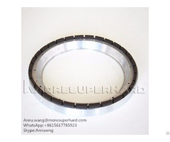
 Back Grinding Wheels For Gan WaferEquipment - Abrasives - more super hard product comapny - China - April 17, 2018 - 1.00 Dollar US$
Back Grinding Wheels� ��for GaN Wafer Silicon wafer back grinding wheels Specifications 1.b e used with Japanese, German, American, Korea and Chinese grinders 2.superior grinding performance 3.high cost performance Shape code Profile Sketch Conventiona...
-
 Silicon Wafer Back Grinding WheelsEquipment - Abrasives - more super hard product comapny - China - April 17, 2018 - 1.00 Dollar US$
Silicon wafer back grinding wheels are mainly used for the thinning and fine grinding of the silicon wafer. Coolant: Oil, emulsion workpiece processed: silicon wafer of discrete devices, integrated chips (IC) and virgin, ATM, Melchiorre, Peter Wolter...
-
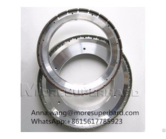
 Silicon Wafer Back Diamond Grinding WheelEquipment - Abrasives - more super hard product comapny - China - April 24, 2018 - 1.00 Dollar US$
Thinning or back grinding wheel Silicon Wafer Back-side Diamond Grinding Wheel Back Grinding W heels for GaN Wafer Silicon wafer back grinding wheels back grinding Wheel for inserts Silicon wafer back grinding wheels are mainly used for the thinning ...
-
 Back Thinning Grinding Wheel For Silicon WaferCutting Tools - more super hard product comapny - China - April 24, 2018 - 1.00 Dollar US$
Thinning or back grinding wheel Silicon Wafer Back-side Diamond Grinding Wheel Back Grinding W heels for GaN Wafer Silicon wafer back grinding wheels back grinding Wheel for inserts Silicon wafer back grinding wheels are mainly used for the thinning ...
-
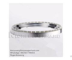
 Vitrified Diamond Grinding Wheels For Top And Bottom Of Sapphire Wafer EdgeEquipment - Abrasives - more super hard product comapny - China - December 13, 2018 - 1.00 Dollar US$
Vitrified Diamond And CBN Grinding Wheels For Top And Bottom Grinding Of Sapphire Wafer Edge Vitrified bond diamond grinding wheels are usually used for sapphire wafer edge grinding. The double disc surface grinding wheel is mainly used to process va...
-
 Cast Steel Wafer Type Butterfly ValvesGeneral Equipment / Machinery - Dervos Forged Steel Valve Manufacturing Co., Ltd - China - December 24, 2018 - contact company for price
Type: Cast Steel Wafer Type Butterfly Valve. Body Material: Cast Steel. Valve Size: 2 Inch. Applicable Pressure Rating: Class 300 LB. Working Temperature: -15℃ to +120℃. Molding Style: Casting. Butterfly Valves can be used for special applications li...
-
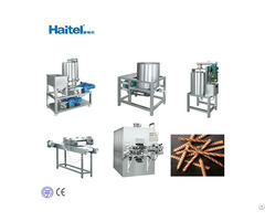 Shanghai Full Automatic Chocolate Egg Roll Wafer Stick Snack Food Making MachineEquipment - Food Processing - Candy / Snack Food - Jiangsu Haitel Machinery Co.,Ltd - China - June 19, 2019 - 35000.00 Dollar US$
1. introduction: egg roll production unit is composed of storing barrels, transmission liquid machines, liquid barrels, color machine, 360 ° rotating auto-baked round, shovel device and the automatic roll feed cutting and electrical control cabinet, ...
-
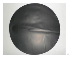 Wafer Pad SupplierElectronics - Electrical Tape - Zhuhai Tongxi Electronics Technology Co., Ltd. - China - November 5, 2019 - contact company for price
Wafer Pad Antistatic Sheets Black Wafer Spacers Information: Wafer pads are also known as antistatic pads, antistatic sheets, conductive separators, black wafer spacers, antistatic wafer spacers, conductive wafer spacers, wafer spacers, black wafer p...
-
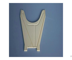 Alumina Ceramic Wafer Loader ArmGeneral Manufacturing - Shanghai Sencer Precision Ceramics Co.,ltd - China - January 3, 2020 - check with company for price
Application: Semiconductor Ceramic, Structure Ceramic, Wear resistant.Excellent abrasive, heat, corrosion-resistance and electrical insulating enable ceramic to be the most widely used material in produing both precision segments and large mechanical...
-
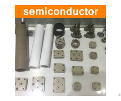 Peek Parts In Semiconductor Part Polymer Components Fittings Wafer Clamp Led Lcd Support Head PlugsPlastic Products - Taizhou Ark International Co.,Ltd - China - April 4, 2020 - contact company for price
peek, pi has the characteristics of high temperature resistance, corrosion resistance, wear resistance, high purity and other advantages. it can fully meet the harsh production environments of electronic semiconductor industry. ensuring its long-time...