Premium listings
-
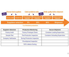 Ningbo Inspection Service Quality Control Of Textile Electronics Blender KettleBusiness - Agent - Eagle Eyes China Inspection Company - China - April 22, 2024 - 198.00 Dollar US$
Common Products Inspected in our Ningbo Inspection Service and Ningbo Quality Control Service: Textile, machinery, metallurgy, electronics, building materials, TV bracket, Flashlight, lamp, Blender, kettle, heaters, Hair dryer, Bike racks, Fireplace,...
-
 Shantou Quality Control Inspection Check Of Drone Toys In Guangdong ProvinceServices - Consulting - Eagle Eyes China Inspection Company - China - April 22, 2024 - 198.00 Dollar US$
Common Products Inspected in our Shantou Inspection Service and Shantou Quality Control Service: food candy, garment, headphone, speaker, toys, pajamas, Bra, plastic products, medicine, machinery, printing package, electronic information devices, aud...
acoustic devices silicon wafer Photos Catalog - WorldBid B2B Market
-
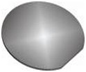
 Acoustic Devices On Silicon WaferGeneral Electronics - Jinan Jingzheng Electronics Co., Ltd. - China - March 30, 2013 - contact company for price
The need for high-frequency, wide-band filters has instigated many developments based on combining thin piezoelectric films and high acoustic velocity materials to ease the manufacture of devices operating above 2 GHz. In the present work, a technolo...
-
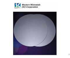
 Cz Fz Diode Grade Silicon WaferComponents - Other - Western Minmetal (SC) Corporation - China - May 30, 2014 - contact company for price
Conductivity: N type or P type Orientation: <100> +/ - 1 degree Resistivity: 5- 100 RRV: 10% , 12% or 25% Diameter: 3”4” 5” Thickness: ( 200- 600) +/ - 5µm Primary Flat: <110>+/ - 1º Length 32.5+/ - 1.5mm Secondary Flat: 180 degree from p...
-
 Fz Ntd Single Crystal Silicon WaferComponents - Other - Western Minmetal (SC) Corporation - China - August 14, 2014 - contact company for price
No. Item Standard Specification 1 Diameter 2” 3” 4” 5” 6” 2 Conductivity Type P/ Boron, N/ Phosphorus 3 Orientation <100><111>±2 ° 4 Thickness μ m 200- 2000( ±5 or ±10) 5 Resistivity Ω . cm 15- 600 6 RRV % ≤ 8 ≤ 10 &...
-
Cz Single Crystal Silicon WaferComponents - Other - Western Minmetal (SC) Corporation - China - August 14, 2014 - contact company for price
No. Item Standard Specification 1 Diameter 2” 3” 4” 6” 8” 2 Conductivity Type P/ Boron, N/ Phosphorus 3 Orientation <110>±1° , <100>±1° 4 Diameter mm 50.8±0.2 76.2±0.2 100±0.3 154±0.3 200±0.3 5 Thickness μ m 180- 1000 6 Resistivity &...
-
 Mcz Single Crystal Silicon WaferComponents - Other - Western Minmetal (SC) Corporation - China - August 14, 2014 - contact company for price
No. Item Standard Specification 1 Diameter mm 76.2- 200 ( 3” 4” 5’ 6” 8”) 2 Conductivity Type P/ Boron, N/ Phosphorus 3 Orientation <100>, <110>, <111> 4 Thickness μ m 180- 1000±20, or as customer required 5 Resistivity Ω ...
-
 Single Crystal Silicon Bonding WaferComponents - Other - Western Minmetal (SC) Corporation - China - August 14, 2014 - contact company for price
No. Item Standard Specification 1 Diameter 2” 4” 2 Conductivity Type P/ Boron, N/ Phosphorus 3 Resistivity Ω . cm ≤ 0.0015 4 Diameter mm 50.8±0.2 100±0.3 5 Thickness μ m 425±25 625±25 6 Orientation 7 Primary length mm 16±1 32±2 8 TTV/...
-
 Cz Fz Diode Silicon WaferComponents - Other - Western Minmetal (SC) Corporation - China - August 14, 2014 - contact company for price
No. Item Standard Specification 1 Diameter3” 4” 2 Conductivity Type 3 Growth method 4 Resistivity Ω . cm 5 Diameter mm 76.2±0.3 100±0.5 6 Thickness μ m 7 Orientation 8 TTV μ m 9 Bow/ Warp μ m 10 RRV % 11 Oxygen a/ cm3 12 Carbon a/...
-
 Fz Single Crystal Silicon WaferComponents - Other - Western Minmetal (SC) Corporation - China - August 14, 2014 - contact company for price
No. Item Standard Specification 1 Diameter mm 53- 150±0.2( 2” 3” 4” 5” 6”) 2 Conductivity Type P/ Boron, N/ Phosphorus 3 Resistivity Ω . cm 10- 150 or as required 4 Orientation 5 Thickness μ m 6 Oxygen ppam 7 Carbon ppam 8 TTV/ TIR μ m...
-
 Monocrystal Silicon Solar WaferComponents - Other - Western Minmetal (SC) Corporation - China - August 14, 2014 - contact company for price
No. Item Standard specification 1 Wafer Square Side 125x125±0.5mm 156x156±0.5 mm 2 Diagonal Length 150±0.5mm 200±0.5mm 3 Growth Method CZ CZ 4 Conductivity Type 5 Shape Wafer 6 Surface Orientation 7 Dislocation 8 Resistivity 9 Lifetime 10 Carbon Cont...
-
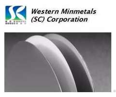
 Cz Single Crystal Silicon Wafer 2 Inch 3 Inch 4 Inch 6 Inch 8 InchComponents - Other - Western Minmetal (SC) Corporation - China - December 24, 2017 - 1.00 Dollar US$
Diameter: 2"3"4"6"8" Growing Method: CZ Conductivity: N type or P type Crystal Orientation: <100> <110>+/-1degree Res istivity: 0.003-80 Ohm.cm RRV: 8% 10% 12% max Thickness: 180-1, 000um Primary Flat / Length: <110>+/-1degree, 16+/...
-
 Fz Single Crystal Silicon Wafer 2 Inch 3 4 6 8Components - Other - Western Minmetal (SC) Corporation - China - December 24, 2017 - 1.00 Dollar US$
FZ Single Crystal Silicon Wafer 2" 3” 4” 5" 6” at Western Minmetals (SC) Corporation Diameter: 2"3"4”5”6” Conducti vity Type: N type or P type Crystal Orientation: <100>, <111> Resistivity: 10-150 Ohm.cm RRV: 20% 25% max Thickness: 325, 3...
-
 Fz Ntd Single Crystal Silicon Wafer 2 Inch 3 Inch 4 Inch 5 Inch 6 Inch At Western Minmetals Sc CorpoComponents - Other - Western Minmetal (SC) Corporation - China - December 24, 2017 - 1.00 Dollar US$
Diameter: 2"3"4”5”6” Conducti vity: N type or P type Crystal Orientation: <100> <111> +/-2degree Resistivity: 15-600 Ohm.cm RRV: 6% 8% 10% 12% max Thickness: 325, 375, 425, 525, 625, 1, 000um, or as required TTV: 10um max, Bow: 10um max, ...
-
 Single Crystal Silicon Prime Test Wafer 2 Inch 3 Inch 4 Inch 5 Inch 6 Inch 8 Inch At Western MinmetaComponents - Other - Western Minmetal (SC) Corporation - China - December 24, 2017 - 1.00 Dollar US$
Diameter: 2" 3" 4" 5” 6” 8" Conductivity Type: N type or P type Crystal Orientation: <100>, <111>, <110>+/-0.5degree R esistivity: 2.0-4.0 Ohm.cm, 4.0-7.0 Ohm.cm, 7.5-12.5 Ohm.cm RRV: 12% max Thickness: 350+/-15um, 420+/-20um, 525+/...
-
 Single Crystal Silicon Epi Wafer 4 Inch 6 Inch 8 Inch At Western Minmetals Sc CorporationComponents - Other - Western Minmetal (SC) Corporation - China - December 24, 2017 - 1.00 Dollar US$
Single Crystal Silicon EPI Wafer 4" 6" 8" at Western Minmetals (SC) Corporation Diameter: 4" 6" 8" Substrate Layer Growth Method: CZ MCZ FZ Dopant: Boron / Phosphorus Conductivity Type: P / N Crystal Orientation: <100> <111> Thickness: 51...
-
 Silicon Soi Wafer 4 Inch 6 Inch 8 Inch At Western Minmetals Sc CorporationComponents - Other - Western Minmetal (SC) Corporation - China - December 24, 2017 - 1.00 Dollar US$
Silicon SOI Wafer 4" 6" 8" at Western Minmetals (SC) Corporation Diameter: 4" 6" 8" Handle Substrate Layer Growth Method: CZ MCZ FZ Conductivity Type: N type or P type Crystal Orientation: <100> <111> Resistivity: 1, 000 Ohm.cm min or as ...
-
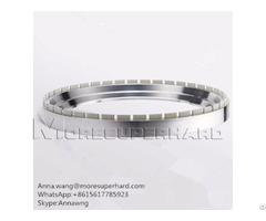
 Silicon Wafer Back Side Diamond Grinding WheelEquipment - Abrasives - more super hard product comapny - China - April 17, 2018 - 1.00 Dollar US$
Back Grinding Wheels Back Grinding Wheels Are Used For The Thinning And Fine Grinding Of The Silicon Wafer. Name: Diamond Backgrinding Wheel Application: Silicon WaferDiamond Back Grinding Wheels Are Used For Silicon Wafer Grinding. Our Advanced Tech...
-
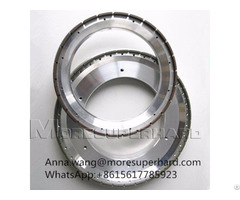
 Silicon Wafer Back Grinding WheelsEquipment - Abrasives - more super hard product comapny - China - April 17, 2018 - 1.00 Dollar US$
Silicon wafer back grinding wheels are mainly used for the thinning and fine grinding of the silicon wafer. Coolant: Oil, emulsion workpiece processed: silicon wafer of discrete devices, integrated chips (IC) and virgin, ATM, Melchiorre, Peter Wolter...
-
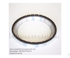
 Silicon Wafer Back Diamond Grinding WheelEquipment - Abrasives - more super hard product comapny - China - April 24, 2018 - 1.00 Dollar US$
Thinning or back grinding wheel Silicon Wafer Back-side Diamond Grinding Wheel Back Grinding W heels for GaN Wafer Silicon wafer back grinding wheels back grinding Wheel for inserts Silicon wafer back grinding wheels are mainly used for the thinning ...
-
 Back Thinning Grinding Wheel For Silicon WaferCutting Tools - more super hard product comapny - China - April 24, 2018 - 1.00 Dollar US$
Thinning or back grinding wheel Silicon Wafer Back-side Diamond Grinding Wheel Back Grinding W heels for GaN Wafer Silicon wafer back grinding wheels back grinding Wheel for inserts Silicon wafer back grinding wheels are mainly used for the thinning ...
-
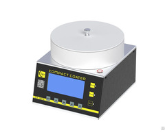 Compact Desktop Spin Coater With Ptfe Chamber For Silicon Wafer CoatingEquipment - Scientific - Zhengzhou CY Scientific Instrument Co., Ltd. - China - July 16, 2020 - 2300.00 Dollar US$
This type of spin coater is designed small, and the whole body adopts aluminum alloy structure. The upper cover of the chamber is made of PTFE, and the appearance is beautiful and firm. The spin coater adopts advanced precision motor, the maximum spe...