crystal silicon bonding wafer Photos Catalog - WorldBid B2B Market
-
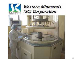
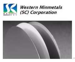
 Single Crystal Silicon Bonding WaferComponents - Other - Western Minmetal (SC) Corporation - China - August 14, 2014 - contact company for price
No. Item Standard Specification 1 Diameter 2” 4” 2 Conductivity Type P/ Boron, N/ Phosphorus 3 Resistivity Ω . cm ≤ 0.0015 4 Diameter mm 50.8±0.2 100±0.3 5 Thickness μ m 425±25 625±25 6 Orientation 7 Primary length mm 16±1 32±2 8 TTV/...
-
 Bf33 Glass Silicon Wafer Bonding Material 0 7 1 0mmLenses / Optical Components - GuangZhou Lighting Glass Co.,Ltd. - China - February 26, 2025 - contact company for price
BF33 Glass, available in thicknesses of 0.7mm and 1.0mm, is a high-quality optical glass designed for silicon wafer bonding applications. This glass offers excellent thermal stability, low thermal expansion, and high transparency, making it an ideal ...
-
 Fz Ntd Single Crystal Silicon WaferComponents - Other - Western Minmetal (SC) Corporation - China - August 14, 2014 - contact company for price
No. Item Standard Specification 1 Diameter 2” 3” 4” 5” 6” 2 Conductivity Type P/ Boron, N/ Phosphorus 3 Orientation <100><111>±2 ° 4 Thickness μ m 200- 2000( ±5 or ±10) 5 Resistivity Ω . cm 15- 600 6 RRV % ≤ 8 ≤ 10 &...
-
 Cz Single Crystal Silicon WaferComponents - Other - Western Minmetal (SC) Corporation - China - August 14, 2014 - contact company for price
No. Item Standard Specification 1 Diameter 2” 3” 4” 6” 8” 2 Conductivity Type P/ Boron, N/ Phosphorus 3 Orientation <110>±1° , <100>±1° 4 Diameter mm 50.8±0.2 76.2±0.2 100±0.3 154±0.3 200±0.3 5 Thickness μ m 180- 1000 6 Resistivity &...
-
 Mcz Single Crystal Silicon WaferComponents - Other - Western Minmetal (SC) Corporation - China - August 14, 2014 - contact company for price
No. Item Standard Specification 1 Diameter mm 76.2- 200 ( 3” 4” 5’ 6” 8”) 2 Conductivity Type P/ Boron, N/ Phosphorus 3 Orientation <100>, <110>, <111> 4 Thickness μ m 180- 1000±20, or as customer required 5 Resistivity Ω ...
-
 Fz Single Crystal Silicon WaferComponents - Other - Western Minmetal (SC) Corporation - China - August 14, 2014 - contact company for price
No. Item Standard Specification 1 Diameter mm 53- 150±0.2( 2” 3” 4” 5” 6”) 2 Conductivity Type P/ Boron, N/ Phosphorus 3 Resistivity Ω . cm 10- 150 or as required 4 Orientation 5 Thickness μ m 6 Oxygen ppam 7 Carbon ppam 8 TTV/ TIR μ m...
-
 Cz Single Crystal Silicon Wafer 2 Inch 3 Inch 4 Inch 6 Inch 8 InchComponents - Other - Western Minmetal (SC) Corporation - China - December 24, 2017 - 1.00 Dollar US$
Diameter: 2"3"4"6"8" Growing Method: CZ Conductivity: N type or P type Crystal Orientation: <100> <110>+/-1degree Res istivity: 0.003-80 Ohm.cm RRV: 8% 10% 12% max Thickness: 180-1, 000um Primary Flat / Length: <110>+/-1degree, 16+/...
-
 Fz Single Crystal Silicon Wafer 2 Inch 3 4 6 8Components - Other - Western Minmetal (SC) Corporation - China - December 24, 2017 - 1.00 Dollar US$
FZ Single Crystal Silicon Wafer 2" 3” 4” 5" 6” at Western Minmetals (SC) Corporation Diameter: 2"3"4”5”6” Conducti vity Type: N type or P type Crystal Orientation: <100>, <111> Resistivity: 10-150 Ohm.cm RRV: 20% 25% max Thickness: 325, 3...
-
 Fz Ntd Single Crystal Silicon Wafer 2 Inch 3 Inch 4 Inch 5 Inch 6 Inch At Western Minmetals Sc CorpoComponents - Other - Western Minmetal (SC) Corporation - China - December 24, 2017 - 1.00 Dollar US$
Diameter: 2"3"4”5”6” Conducti vity: N type or P type Crystal Orientation: <100> <111> +/-2degree Resistivity: 15-600 Ohm.cm RRV: 6% 8% 10% 12% max Thickness: 325, 375, 425, 525, 625, 1, 000um, or as required TTV: 10um max, Bow: 10um max, ...
-
 Single Crystal Silicon Prime Test Wafer 2 Inch 3 Inch 4 Inch 5 Inch 6 Inch 8 Inch At Western MinmetaComponents - Other - Western Minmetal (SC) Corporation - China - December 24, 2017 - 1.00 Dollar US$
Diameter: 2" 3" 4" 5” 6” 8" Conductivity Type: N type or P type Crystal Orientation: <100>, <111>, <110>+/-0.5degree R esistivity: 2.0-4.0 Ohm.cm, 4.0-7.0 Ohm.cm, 7.5-12.5 Ohm.cm RRV: 12% max Thickness: 350+/-15um, 420+/-20um, 525+/...
-
 Single Crystal Silicon Epi Wafer 4 Inch 6 Inch 8 Inch At Western Minmetals Sc CorporationComponents - Other - Western Minmetal (SC) Corporation - China - December 24, 2017 - 1.00 Dollar US$
Single Crystal Silicon EPI Wafer 4" 6" 8" at Western Minmetals (SC) Corporation Diameter: 4" 6" 8" Substrate Layer Growth Method: CZ MCZ FZ Dopant: Boron / Phosphorus Conductivity Type: P / N Crystal Orientation: <100> <111> Thickness: 51...
-
 Cz Fz Diode Grade Silicon WaferComponents - Other - Western Minmetal (SC) Corporation - China - May 30, 2014 - contact company for price
Conductivity: N type or P type Orientation: <100> +/ - 1 degree Resistivity: 5- 100 RRV: 10% , 12% or 25% Diameter: 3”4” 5” Thickness: ( 200- 600) +/ - 5µm Primary Flat: <110>+/ - 1º Length 32.5+/ - 1.5mm Secondary Flat: 180 degree from p...
-
 Cz Fz Diode Silicon WaferComponents - Other - Western Minmetal (SC) Corporation - China - August 14, 2014 - contact company for price
No. Item Standard Specification 1 Diameter3” 4” 2 Conductivity Type 3 Growth method 4 Resistivity Ω . cm 5 Diameter mm 76.2±0.3 100±0.5 6 Thickness μ m 7 Orientation 8 TTV μ m 9 Bow/ Warp μ m 10 RRV % 11 Oxygen a/ cm3 12 Carbon a/...
-
 Monocrystal Silicon Solar WaferComponents - Other - Western Minmetal (SC) Corporation - China - August 14, 2014 - contact company for price
No. Item Standard specification 1 Wafer Square Side 125x125±0.5mm 156x156±0.5 mm 2 Diagonal Length 150±0.5mm 200±0.5mm 3 Growth Method CZ CZ 4 Conductivity Type 5 Shape Wafer 6 Surface Orientation 7 Dislocation 8 Resistivity 9 Lifetime 10 Carbon Cont...
-
Acoustic Devices On Silicon WaferGeneral Electronics - Jinan Jingzheng Electronics Co., Ltd. - China - March 30, 2013 - contact company for price
The need for high-frequency, wide-band filters has instigated many developments based on combining thin piezoelectric films and high acoustic velocity materials to ease the manufacture of devices operating above 2 GHz. In the present work, a technolo...
-
 Silicon Soi Wafer 4 Inch 6 Inch 8 Inch At Western Minmetals Sc CorporationComponents - Other - Western Minmetal (SC) Corporation - China - December 24, 2017 - 1.00 Dollar US$
Silicon SOI Wafer 4" 6" 8" at Western Minmetals (SC) Corporation Diameter: 4" 6" 8" Handle Substrate Layer Growth Method: CZ MCZ FZ Conductivity Type: N type or P type Crystal Orientation: <100> <111> Resistivity: 1, 000 Ohm.cm min or as ...
-
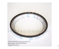 Silicon Wafer Back Side Diamond Grinding WheelEquipment - Abrasives - more super hard product comapny - China - April 17, 2018 - 1.00 Dollar US$
Back Grinding Wheels Back Grinding Wheels Are Used For The Thinning And Fine Grinding Of The Silicon Wafer. Name: Diamond Backgrinding Wheel Application: Silicon WaferDiamond Back Grinding Wheels Are Used For Silicon Wafer Grinding. Our Advanced Tech...
-
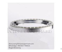 Silicon Wafer Back Grinding WheelsEquipment - Abrasives - more super hard product comapny - China - April 17, 2018 - 1.00 Dollar US$
Silicon wafer back grinding wheels are mainly used for the thinning and fine grinding of the silicon wafer. Coolant: Oil, emulsion workpiece processed: silicon wafer of discrete devices, integrated chips (IC) and virgin, ATM, Melchiorre, Peter Wolter...
-
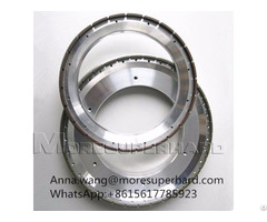 Silicon Wafer Back Diamond Grinding WheelEquipment - Abrasives - more super hard product comapny - China - April 24, 2018 - 1.00 Dollar US$
Thinning or back grinding wheel Silicon Wafer Back-side Diamond Grinding Wheel Back Grinding W heels for GaN Wafer Silicon wafer back grinding wheels back grinding Wheel for inserts Silicon wafer back grinding wheels are mainly used for the thinning ...
-
 Back Thinning Grinding Wheel For Silicon WaferCutting Tools - more super hard product comapny - China - April 24, 2018 - 1.00 Dollar US$
Thinning or back grinding wheel Silicon Wafer Back-side Diamond Grinding Wheel Back Grinding W heels for GaN Wafer Silicon wafer back grinding wheels back grinding Wheel for inserts Silicon wafer back grinding wheels are mainly used for the thinning ...