Premium listings
-
 Ningbo Inspection Service Quality Control Of Textile Electronics Blender KettleBusiness - Agent - Eagle Eyes China Inspection Company - China - April 22, 2024 - 198.00 Dollar US$
Common Products Inspected in our Ningbo Inspection Service and Ningbo Quality Control Service: Textile, machinery, metallurgy, electronics, building materials, TV bracket, Flashlight, lamp, Blender, kettle, heaters, Hair dryer, Bike racks, Fireplace,...
-
 Shantou Quality Control Inspection Check Of Drone Toys In Guangdong ProvinceServices - Consulting - Eagle Eyes China Inspection Company - China - April 22, 2024 - 198.00 Dollar US$
Common Products Inspected in our Shantou Inspection Service and Shantou Quality Control Service: food candy, garment, headphone, speaker, toys, pajamas, Bra, plastic products, medicine, machinery, printing package, electronic information devices, aud...
crystal silicon prime test wafer western minmeta Photos Catalog - WorldBid B2B Market
-
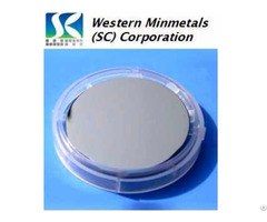
 Single Crystal Silicon Prime Test Wafer 2 Inch 3 Inch 4 Inch 5 Inch 6 Inch 8 Inch At Western MinmetaComponents - Other - Western Minmetal (SC) Corporation - China - December 24, 2017 - 1.00 Dollar US$
Diameter: 2" 3" 4" 5” 6” 8" Conductivity Type: N type or P type Crystal Orientation: <100>, <111>, <110>+/-0.5degree R esistivity: 2.0-4.0 Ohm.cm, 4.0-7.0 Ohm.cm, 7.5-12.5 Ohm.cm RRV: 12% max Thickness: 350+/-15um, 420+/-20um, 525+/...
-
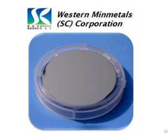
 Fz Ntd Single Crystal Silicon Wafer 2 Inch 3 Inch 4 Inch 5 Inch 6 Inch At Western Minmetals Sc CorpoComponents - Other - Western Minmetal (SC) Corporation - China - December 24, 2017 - 1.00 Dollar US$
Diameter: 2"3"4”5”6” Conducti vity: N type or P type Crystal Orientation: <100> <111> +/-2degree Resistivity: 15-600 Ohm.cm RRV: 6% 8% 10% 12% max Thickness: 325, 375, 425, 525, 625, 1, 000um, or as required TTV: 10um max, Bow: 10um max, ...
-
 Single Crystal Silicon Epi Wafer 4 Inch 6 Inch 8 Inch At Western Minmetals Sc CorporationComponents - Other - Western Minmetal (SC) Corporation - China - December 24, 2017 - 1.00 Dollar US$
Single Crystal Silicon EPI Wafer 4" 6" 8" at Western Minmetals (SC) Corporation Diameter: 4" 6" 8" Substrate Layer Growth Method: CZ MCZ FZ Dopant: Boron / Phosphorus Conductivity Type: P / N Crystal Orientation: <100> <111> Thickness: 51...
-
 Silicon Soi Wafer 4 Inch 6 Inch 8 Inch At Western Minmetals Sc CorporationComponents - Other - Western Minmetal (SC) Corporation - China - December 24, 2017 - 1.00 Dollar US$
Silicon SOI Wafer 4" 6" 8" at Western Minmetals (SC) Corporation Diameter: 4" 6" 8" Handle Substrate Layer Growth Method: CZ MCZ FZ Conductivity Type: N type or P type Crystal Orientation: <100> <111> Resistivity: 1, 000 Ohm.cm min or as ...
-
 Gallium Phosphide Gap Single Crystal Wafer 2 At Western Minmetals Sc CorporationComponents - Other - Western Minmetal (SC) Corporation - China - December 24, 2017 - 1.00 Dollar US$
Diameter: 50.8+/- 0.2 mm Dopant: None / Sulphur Conduct Type: SC/P Growth Method: LEC Thickness: 300+/-20 um Crystal Orientation: <111>+/-0.5degree O rientation Flat / Length: as SEMI Identification Flat / Length: as SEMI Orientation / Identifi...
-
 Gallium Antimonide Gasb Single Crystal Wafer 3 4 At Western Minmetals Sc CorporationComponents - Other - Western Minmetal (SC) Corporation - China - December 24, 2017 - 1.00 Dollar US$
Diameter: 76.2+/- 0.2, 100+/-0.2 mm Dopant: None / Tellurium / Zinc Conduct Type: N / P Growth Method: LEC Thickness: 625+/-25, 1, 000+/-25 um Crystal Orientation: <100> <111>+/-0.5degree O rientation Flat / Length: as SEMI Identification...
-
 Indium Phosphide Inp Single Crystal Wafer 2 3 At Western Minmetals Sc CorporationComponents - Other - Western Minmetal (SC) Corporation - China - December 24, 2017 - 1.00 Dollar US$
Diameter: 50.8+/- 0.2, 76.2+/- 0.2 mm Dopant: None / Sulphur / Ferrum / Zinc Conduct Type: N / P Growth Method: LEC Thickness: 200-2, 000+/-5 or +/-10 um Crystal Orientation: <100> <111> Orientation Flat / Length: as SEMI Identification F...
-
 Indium Antimonide Insb Single Crystal Wafer 2 At Western Minmetals Sc CorporationComponents - Other - Western Minmetal (SC) Corporation - China - December 24, 2017 - 1.00 Dollar US$
Indium Antimonide (InSb) Single Crystal Wafer 2’’ at Western Minmetals (SC) Corporation Diameter: 50.8+/- 0.2 mm Dopant: None / Tellurium / Germanium Conduct Type: N / P Doping Level: > 2E18 /cm2 Growth Method: LEC Thickness: 500+/-25 um Warp: <...
-
 Indium Arsenide Inas Single Crystal Wafer 2 3 At Western Minmetals Sc CorporationComponents - Other - Western Minmetal (SC) Corporation - China - December 24, 2017 - 1.00 Dollar US$
Diameter: 50.8+/- 0.2, 76.2+/- 0.2 mm Dopant: None / Sulphur / Zinc Conduct Type: N / P Doping Level: > 2E18 /cm2 Growth Method: LEC Thickness: 500+/-25 um Warp: < 15 um Crystal Orientation: <100>+/-2degree, <111>+/-2degree, Alpha90...
-
 Fz Ntd Single Crystal Silicon WaferComponents - Other - Western Minmetal (SC) Corporation - China - August 14, 2014 - contact company for price
No. Item Standard Specification 1 Diameter 2” 3” 4” 5” 6” 2 Conductivity Type P/ Boron, N/ Phosphorus 3 Orientation <100><111>±2 ° 4 Thickness μ m 200- 2000( ±5 or ±10) 5 Resistivity Ω . cm 15- 600 6 RRV % ≤ 8 ≤ 10 &...
-
 Cz Single Crystal Silicon WaferComponents - Other - Western Minmetal (SC) Corporation - China - August 14, 2014 - contact company for price
No. Item Standard Specification 1 Diameter 2” 3” 4” 6” 8” 2 Conductivity Type P/ Boron, N/ Phosphorus 3 Orientation <110>±1° , <100>±1° 4 Diameter mm 50.8±0.2 76.2±0.2 100±0.3 154±0.3 200±0.3 5 Thickness μ m 180- 1000 6 Resistivity &...
-
 Mcz Single Crystal Silicon WaferComponents - Other - Western Minmetal (SC) Corporation - China - August 14, 2014 - contact company for price
No. Item Standard Specification 1 Diameter mm 76.2- 200 ( 3” 4” 5’ 6” 8”) 2 Conductivity Type P/ Boron, N/ Phosphorus 3 Orientation <100>, <110>, <111> 4 Thickness μ m 180- 1000±20, or as customer required 5 Resistivity Ω ...
-
 Single Crystal Silicon Bonding WaferComponents - Other - Western Minmetal (SC) Corporation - China - August 14, 2014 - contact company for price
No. Item Standard Specification 1 Diameter 2” 4” 2 Conductivity Type P/ Boron, N/ Phosphorus 3 Resistivity Ω . cm ≤ 0.0015 4 Diameter mm 50.8±0.2 100±0.3 5 Thickness μ m 425±25 625±25 6 Orientation 7 Primary length mm 16±1 32±2 8 TTV/...
-
 Fz Single Crystal Silicon WaferComponents - Other - Western Minmetal (SC) Corporation - China - August 14, 2014 - contact company for price
No. Item Standard Specification 1 Diameter mm 53- 150±0.2( 2” 3” 4” 5” 6”) 2 Conductivity Type P/ Boron, N/ Phosphorus 3 Resistivity Ω . cm 10- 150 or as required 4 Orientation 5 Thickness μ m 6 Oxygen ppam 7 Carbon ppam 8 TTV/ TIR μ m...
-
 Cz Single Crystal Silicon Wafer 2 Inch 3 Inch 4 Inch 6 Inch 8 InchComponents - Other - Western Minmetal (SC) Corporation - China - December 24, 2017 - 1.00 Dollar US$
Diameter: 2"3"4"6"8" Growing Method: CZ Conductivity: N type or P type Crystal Orientation: <100> <110>+/-1degree Res istivity: 0.003-80 Ohm.cm RRV: 8% 10% 12% max Thickness: 180-1, 000um Primary Flat / Length: <110>+/-1degree, 16+/...
-
 Fz Single Crystal Silicon Wafer 2 Inch 3 4 6 8Components - Other - Western Minmetal (SC) Corporation - China - December 24, 2017 - 1.00 Dollar US$
FZ Single Crystal Silicon Wafer 2" 3” 4” 5" 6” at Western Minmetals (SC) Corporation Diameter: 2"3"4”5”6” Conducti vity Type: N type or P type Crystal Orientation: <100>, <111> Resistivity: 10-150 Ohm.cm RRV: 20% 25% max Thickness: 325, 3...
-
 Gallium Arsenide Gaas Si Doped Wafer 2 3 4 At Western Minmetals Sc CorporationComponents - Other - Western Minmetal (SC) Corporation - China - December 24, 2017 - 1.00 Dollar US$
Diameter: 50.8+/- 0.2, 76.2+/-0.3, 100+/-0.3 mm Dopant: Silicon Conduct Type: SC/N Growth Method: VGF Thickness: 220-350+/-20 um Crystal Orientation: <100>+/-0.5degree O rientation Flat / Length: 16+/-1, 22+/-1, 32+/-1 mm Identification Flat / ...
-
 Gallium Arsenide Gaas Zn Doped Wafer 2 3 4 At Western Minmetals Sc CorporationComponents - Other - Western Minmetal (SC) Corporation - China - December 24, 2017 - 1.00 Dollar US$
Diameter: 50.8+/- 0.2, 76.2+/-0.3, 100+/-0.3 mm Dopant: Zinc Conduct Type: SC/P Growth Method: VGF Thickness: 220-350+/-20 um Crystal Orientation: <100>+/-0.5degree O rientation Flat / Length: 16+/-1, 22+/-1, 32+/-1 mm Identification Flat / Len...
-
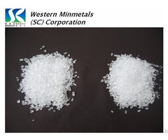 High Purity Silicon Dioxide At Western Minmetals Sio2 99 999 PercentChemicals - Oxide - Western Minmetals (SC) Corporation - China - December 15, 2017 - check with company for price
High Purity Silicon Dioxide is mainly used to produce elemental silicon, optical glass, optical fiber and as coating materials. It is also a primary raw material for elctronic components. 1.SiO2≥99.999% 2.Impuri ty Max each Al/Fe/Pb/Ti/Mg 1ppm, Cr/Mn...
-
 Cz Fz Diode Grade Silicon WaferComponents - Other - Western Minmetal (SC) Corporation - China - May 30, 2014 - contact company for price
Conductivity: N type or P type Orientation: <100> +/ - 1 degree Resistivity: 5- 100 RRV: 10% , 12% or 25% Diameter: 3”4” 5” Thickness: ( 200- 600) +/ - 5µm Primary Flat: <110>+/ - 1º Length 32.5+/ - 1.5mm Secondary Flat: 180 degree from p...